Plasma technology application to PCB/FPCB Industry | PSM

PSM Co., Ltd. has led the development of atmospheric pressure plasma technology through constant technological innovation for more than 20 years since its foundation in 2001. PSM is now leading the global market with the core atmospheric plasma technology based on such accumulated expertise.
Through the technological prowess, PSM has grown into a plasma technology company that is well recognized in the global market as well as in the Korean domestic market of various industries. PSM’s overseas customers located in many countries around world such as China, Japan, Taiwan, USA, and new customers are expanding into Southeast Asia and North America countries. atmospheric pressure plasma technique
With a vision for the new 100 years ahead, PSM will continue to devote itself to research and development and build a more efficient management system through the establishment of the ERP system and the ISO9000 and ISO14000.
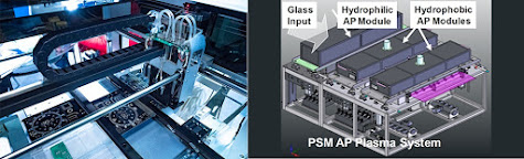
PSM’s various Plasma Application processing in PCB/FPCB Industry
PSM’s AP Plasma M electrode (APM) is applied to the pre-treatment process for PCB substrate plating and the surface treatment process before SMT/Flip-chip bonding and applied to the surface treatment process for flexible PI film substrate and polymer substrate.
It is possible to do Low-temperature processing (below 40 ℃), and it does not require consumable parts.
And AP plasma roll-to-roll equipment is applied to the surface treatment process for FPCB FCCL PI films and vacuum plasma equipment is used in the PCB decontamination process.
Along with such applications, PSM provides vacuum plasma de-smear processing in PCB/FPCB Industry. semiconductor packaging technology korea
ü It
performs the uniform
removal of epoxy residues (smear) generated during the PCB drilling
process and secures product reliability
ü
It consumes a small amount of gas and has a low running cost due to no
chemical disposal
expenses


Comments
Post a Comment