Plasma Application to Display Printing Industry | PSM Korea

PSM Co., Ltd. has led the development of atmospheric pressure plasma technology through constant technological innovation and R&D investment for almost 20 years since its foundation in 2001.
PSM is now leading the global market with its core atmospheric plasma technology based on such a long-time accumulated expertise.
Through the technological prowess, PSM has
grown into a world-class plasma company that
is well recognized in the global market as well as the
Korean domestic market in various industries.
PSM currently possesses lots of patents for its proprietary atmospheric plasma technologies and
will go on to invest in
technological innovation and quality improvement. PSM plans to build a more efficient
management system through the establishment of the ERP system and the ISO9000
and ISO14000. Glass panel cleaning system supplier
PSM plasma technology and equipment application to display printing industry
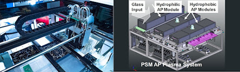
ü PSM plasma Electrode is available applied to OLED RGB /Quantum Dot Display inkjet process:
Applied to the
selective surface treatment process before inkjet printing for the OLED RGB
Pattern /Quantum Dot Display Atmospheric Pressure Plasma Cleaning System
Applied to the Nano-imprinting pre-treatment/primer
removal processes
It can be stably applied to large samples (6~10G) as well to processing
speed at 6-8m/min
ü PSM vacuum plasma is available applied to Descum/Etching for the patterning process:
The PSM vacuum plasma
system uses a unique vacuum and gas flow technology
The best resin
removal system and etching equipment are provided
It is
applied to the Descum process to remove the resin on the substrate surface
It is applied to
glass etching for forming Nano-imprinting
patterns
ü
PSM plasma M/DRP electrode is available applied to
improve the printing process of Gravure printing/screen printing:
Very high
cleaning effect (it has up to 5 time’s higher cleaning effect than the existing
AP)
The gap
between electrode and sample is large (up to 12mm max.)
It can be applied to large sample panels by
connecting DRP electrodes in series.


Comments
Post a Comment