PSM Solar Cell/Industrial Sunglasses Environmentally Friendly DRP Uses

Since its foundation in 2001, PSM has led the development of atmospheric plasma technology through constant technological innovation for the past 20 years. With unwavering faith in following principles while not being afraid of change, we have overcome limitations of plasma technology step by step. Through the technological prowess, we are growing into a plasma company that is recognized in the global market as well as the Korean semiconductor industry.
With a vision for the new 100 years ahead, PSM will use 2020
as the year of development and growth in order to continue to promote new
changes and innovations, and pursue the following changes and innovations. semiconductor
packaging technology
First, we will leap forward as a global company by expanding
the sales network in overseas markets such as China, Taiwan, Japan, and USA as
well as application fields such as the domestic semiconductor, display, and
film markets.
Second, as a leader of the atmospheric plasma
commercialization technology both in Korea and overseas, we currently possess
patents for core atmospheric plasma technologies, and will secure more patented
technologies through continuous development of technology. Also, we will
continue to invest in technological innovation and quality improvement by
strengthening the technology innovation group and the QC sector.
Third, we plan to build a more efficient management system
through establishment of the ERP system, and ISO9000 and ISO14000.
Solar Cell/Industrial Sunglasses:
·
It reduces the concentration of chemicals by
applying a DRP electrode to thin-film solar cell chemical cleaning process
(environmentally friendly)
·
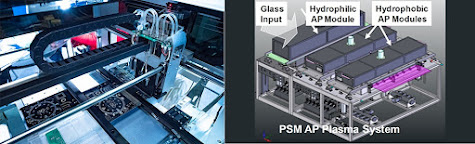
Apply AP plasma (DRP electrode) by pre-treatment
of smart glass (architecture glass) coating
DRP:
·
It can reduce the chemical concentration in the
chemical (alkaline) cleaning process (environmentally friendly) wet cleaning system
manufacturer
·
It improves the production yield by increasing
reliability of thin-film coating
·
Cleaning the contaminated glass substrate (Solar
Cell Panel, and Smart Glass)
·
It can remove suction marks, pin marks, water
marks on displays, architectural glass panels, and so on
·
It can remove residues of nano coating film used
to protect the surface such as AF
AP plasma (M electrode) is applied to the
texturing/diffusion pre-treatment processes for crystalline silicon solar cells


Comments
Post a Comment