PSM Semiconductor Packaging Applications of NPT303-230S Encap/Molding module

PSM Plasma Systems is global leader plasma technology for
Semiconductor, PCB, LCD and Material industries.
We PSM Inc. has rich experience and excellent staffs who
have developed and commercialized various highly evaluated optimized processing
techniques and practical manufacturing systems which are related to
Semiconductor & Display industry, PCB & FCCL industry and other polymer
industries o ver 10 years in the Institute for Advanced Engineering.
The atmospheric pressure plasma technique is a new advanced
plasma system, which can overcome the limit of existing low-pressure vacuum plasma
technique.
This is indeed useful technique that is able to improve
productivity and quality simultaneously not only for
semiconductor/displays/electronic parts, but for low-temperature material
industry such as polymer & plastic / FPCB & FCCL by a possible in-line
process. We PSM Inc. are expanding and
thriving based on the diverse world-leading essential patents of atmospheric
pressure plasma techniques throughout the following four areas: semiconductor
packaging/display dry cleaning/polymer materials, surface treatments
/environmental system; furthermore, our technology has acquired a reputation in
a wide range of areas. semiconductor
packaging technology Korea
Semiconductor packaging Applications:
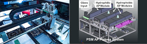
AP (Atmospheric Pressure) Plasma System
Can treat substrate automatic in-line process.
PSM NPT series AP plasma system is applicable for whole
back-end line of semiconductor packaging.
This NPT series provides good uniformity and process
consistency.
PSM AP plasma module
can be directly installed on the wire bonding / molding system. No extra
operation step is needed and in-line continuous process is possible.
Especially MCP (Multi-Chip Package) and fine pitch wire
bonding devices, vacuum plasma cause substrate damage possible by repeat
treatment, but AP plasma no damage and good process quality.
Encap. / Molding Module
Major Applications:
Pre-treatment before Encap. /Molding process to decrease the die-top delamination.
Specifications:
·
Electrode Size: 220mm(W) x 120mm(D) x 45(80)
mm(H)
·
Power Supply Size: 266mm(W) x 605mm(D) x
482mm(H)
·
Plasma Treatment Time: 5 ~ 10 sec (depend on
Substrate)
·
Utility: N2(~ 20 l/min), Air(~100sccm)
·
Application Substrate: BGA, QFN
System Features:
·
In-Line process (AP Module + Molding Machine)
·
Substitute Present Vacuum Plasma Cleaning System
Support In-Line Process, Increase UPH
·
No Surface Damage, Process consistency
·
Easy Installation and Simple Operation with
Convenient Maintenance


Comments
Post a Comment