PSM NPT series AP plasma system and Flip-chip BGA package in Korea

PSM Plasma Systems is global leader plasma technology for
Semiconductor, PCB, LCD and Material industries.
We PSM Inc. has rich experience and excellent staffs who
have developed and commercialized various highly evaluated optimized processing
techniques and practical manufacturing systems which are related to
Semiconductor & Display industry, PCB & FCCL industry and other polymer
industries over 10 years in the Institute for Advanced Engineering.
Semiconductor Packaging Applications
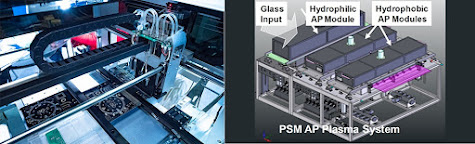
AP (Atmospheric Pressure) Plasma System Can treat substrate
automatic in-line process. PSM NPT series AP plasma system is applicable for whole
back-end line of semiconductor packaging. This NPT series provides good
uniformity and process consistency. atmospheric pressure plasma
technique
Die attach (NPT303-70s-k)
This AP system is attached by die attach epoxy print machine
(screen print machine). Plasma cleaning improves between die attach epoxy and
substrate, namely increase reliability.
Wire Bonding / molding(NPT 305S / NPT 303-230S)
PSM AP plasma module can be directly installed on the wire
bonding / molding system. No extra operation step is needed and in-line
continuous process is possible.
Especially MCP (Multi-Chip Package) and fine pitch wire
bonding devices, vacuum plasma cause substrate damage possible by repeat
treatment, but AP plasma no damage and good process quality
Ball missing of BGA package (NPT 301)
The surface contamination after molding & cure increase
the missing ball by thousands ppm.
NPT301 is a dual head AP plasma and therefore increase the
throughput. Moreover, the system can be configured for dual-line
magazine-to-magazine process. Ap Plasma System
Manufacturer
Flip-chip BGA Process (NPT304-120S)
Flip-chip BGA package substrate is cleaned using plasma to
increase flux wet ability for improvement of adhesion
property of flip-chip bonding & under fill.
Vacuum Plasma System
Die attach/ Wire Bonding /molding / Ball missing of
BGA package (NPT-V01, NPT-v04)
The NPT-V01 plasma system is widely used for the
surface cleaning and modification process of semiconductor packaging and
material treating. The demand of smaller chip size and fine pattern bring about
the critical issues of semiconductor packaging.
PSM NPT-V01 plasma system has been applied the treatment of
semiconductor back-end process, die attach and wire bonding, molding, ball
mount.
PSM designed NPT-V04 to improve above issues by using Dual
Power Supply
Dual Power Supply make minimized Collisional Ion Energy and
Wire Short issue can be solved by minimized Collision Ion Energy.


Comments
Post a Comment