PSM Atmospheric Pressure Plasma Cleaning System for Plating Pretreatment of PCB

PSM Plasma Systems is global leader plasma technology for
Semiconductor, PCB, LCD and Material industries.
We PSM Inc. has rich experience and excellent staffs who
have developed and commercialized various highly evaluated optimized processing
techniques and practical manufacturing systems which are related to
Semiconductor & Display industry, PCB & FCCL industry and other polymer
industries over 10 years in the Institute for Advanced Engineering.
The atmospheric pressure plasma technique is a new advanced
plasma system, which can overcome the limit of existing low-pressure vacuum
plasma technique. Surface treatment System Korea
This is indeed useful technique that is able to improve
productivity and quality simultaneously not only for
semiconductor/displays/electronic parts, but for low-temperature material
industry such as polymer & plastic / FPCB & FCCL by a possible in-line
process. We PSM Inc. are expanding and thriving based on the diverse
world-leading essential patents of atmospheric pressure plasma techniques
throughout the following four areas: semiconductor packaging/display dry
cleaning/polymer materials, surface treatments /environmental system;
furthermore, our technology has acquired a reputation in a wide range of areas.
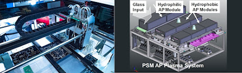
PCB Applications:
PCB (NPT306):
Fine Pitch is the latest trend in PCB Substrate. Fine Pitch
(Smaller Circuit Width, Circuit Gap and Ball Pad Size) have caused increased
failure such as Pit Failure, Wetting Failure, Organic Residual Remove and
Surface Cleaning. These issues have led to increased requirement for plasma
processing. Wet cleaning system
manufacturer
Feature:
Small Size, Easy to
Installation
·
Able to insert with the existing manufacturing
line as “Console Type”
·
Able to install on the existing equipment as
“Add-on Type”
·
Make efficient use of clean room space
Substitution for
conventional Vacuum Plasma system
·
Cut down the labor cost
·
Increased productivity by automated distribution
Increased production
efficiency
·
Decreased failure rate by conventional Wet
Process + Atmospheric Plasma process
Various applications
PSM Atmospheric Plasma Cleaning System is able to apply for every PCB manufacturing process such as
Memory Module PCB, Semiconductor Package Substrate, and Telecommunications
Board etc. So, these neutral radicals can be very effectively used for cleaning
and various surface treatment processes without any surface damage problems.


Comments
Post a Comment