Introduction of PSM Plasma Technology for Material Industries in Korea

PSM Plasma Systems is global leader plasma technology for
Semiconductor, PCB, LCD and Material industries.
We PSM Inc. has rich experience and excellent staffs who
have developed and commercialized various highly evaluated optimized processing
techniques and practical manufacturing systems which are related to
Semiconductor & Display industry, PCB & FCCL industry and other polymer
industries over 10 years in the Institute for Advanced Engineering.
The atmospheric pressure plasma technique is a new advanced
plasma system, which can overcome the limit of existing low-pressure vacuum
plasma technique.
This is indeed useful technique that is able to improve
productivity and quality simultaneously not only for
semiconductor/displays/electronic parts, but for low-temperature material
industry such as polymer & plastic / FPCB & FCCL by a possible in-line
process. We PSM Inc. are expanding and
thriving based on the diverse world-leading essential patents of atmospheric
pressure plasma techniques throughout the following four areas: semiconductor
packaging/display dry cleaning/polymer materials, surface treatments /environmental
system; furthermore, our technology has acquired a reputation in a wide range
of areas. atmospheric pressure plasma
System manufacturer
What is atmospheric pressure plasma?
Atmospheric pressure plasma discharge system requires no
vacuum systems and chambers, because using specially designed electrode and
power sources technique, the plasma can be easily generated at 1atm (760 torr).
So, it could be the best solution for the company which requires
continuous in-line plasma processing for mass production.
We use special dielectric materials and electrode design to
obtain more effective breakdown voltage between two opposite electrodes. Gases
between electrodes become ionized into active neutral radicals, ions and
electrons under carefully biased AC voltage. Among these particles, active
neutral radicals are very reactive and, the density of them are very high as
much as 100~1000 times comparing to conventional vacuum plasma particles. Semiconductor
Packaging Technology
So, these neutral radicals can be very effectively used for
cleaning and various surface treatment processes without any surface damage
problems.
Main Products:
·
Atmospheric pressure Plasma (APP)
·
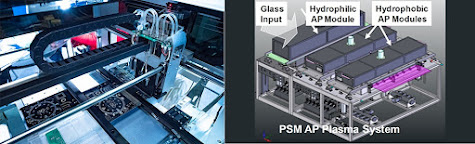
Glass Panel Cleaning System for Flat panel
Display
·
Surface treatment System for Semiconductor packaging
and PCB
·
Environment Plasma System
·
Vacuum Plasma Cleaner


Comments
Post a Comment